Rebuilding bridges - An MSCA contingency plan: the lifeguard during the pandemic
Newsletter
How the contingency plan is serving as an international hub for the advancement of semiconductor scaling.
The MSCA framework
The Marie Skłodowska-Curie Action (MSCA) programme supports innovative and groundbreaking ideas that would potentially benefit society and the career of the applicants. These ideas are included in a meticulous proposal that defines the execution of the action. Work packages, objectives, milestones and potential results are carefully described. The project should include a contingency plan – this is the part which is usually not so extensive and could even go unnoticed. Probably, no one could have anticipated the global pandemic while writing the contingency plan of an MSCA two years ago (or at least, I couldn't have).
However, reality exceeds fiction, and here we are. Now, the contingency plan has become the project’s lifeguard for some of us. Additionally, in my case, it has also resulted in a wider collaboration than initially planned.
The project and the COVID-19 pandemic
The MSCA project, Understanding The Role of the defects to Accomplish High Performance and Stable Two Dimensional Devices (TRAPS-2D), aims to fabricate semiconductor devices employing novel two-dimensional (2D) materials. These 2D materials are single-atom-thick layers whose electrical properties allow us to perform more scalable, reliable and powerful circuits and chips. MSCA Global fellowships require an outgoing phase and we have chosen Taiwan, the unmatched leader of the global semiconductor industry. However, the pandemic and the subsequent lockdown threatened the outgoing phase from the very beginning.
After the initial chaos of the pandemic and the end of the initial lockdown, things seemed to be improving with the incidence low enough to plan how to launch the action. Moreover, by these dates, the pandemic in Taiwan was under control, thanks to the prompt response of the local government. With all the parameters looking favourable, we started the action. The initial delay to get the visa was compensated by starting the project remotely, fabricating devices in the host institution laboratory, and holding online supervision meetings.
Delta variant and the Contingency Plan
Once the visa was obtained and the flights and the quarantine hotel stays were booked, and as I was almost getting ready to proceed with our outgoing phase part of the project, the Delta variant of COVID-19 suddenly surged and struck India and other nearby Asian countries. As a result, on the advice of the Taiwan Centers for Disease Control, Taiwan's Government suspended the entrance for foreign nationals who do not hold a valid resident certificate. These measures aimed to block the spread of the virus, but they blocked me too.
At that time, there were just two possibilities: one option was to ask for a break in the project until the situation would improve and, the second one was to activate the contingency plan. The first solution would have dismantled the previous work. The remote supervision was working perfectly with promising initial results, in both the sample fabrication and characterisation. Breaking the project and putting the action apart for an uncertain period of time would have weakened the novelty of the project and damaged the originality of the results. The second option was risky because the contingency plan did not initially cover the consequences of a global pandemic but, at least, it allowed us to keep the project goals in mind. It consists of fabrication of the samples in the host institution and then sending devices to be processed in Taiwan and in other state-of-the-art semiconductor centers in Europe to increase the chances of success. Our recent collaboration with Paul Hurley’s group at Tyndall National Institute, Ireland, perfectly aligned with the contingency plan requirements. In order to fulfil the action objectives, I would initially receive the planned training in Ireland while some samples could be remotely processed in Taiwan. Despite the possible risks of this latter alternative, we decided to adapt the contingency plan to the pandemic with the support of our collaborators and the approval of the project officer.
Wider international collaboration and results
Fortunately, what seemed a dead-end has become a three-party international collaboration in the race for semiconductor scaling. While I am waiting to visit Taiwan after the COVID-19 incidence reduces, this incipient collaboration has brought impressive advances in our project. At the host institution, we have successfully synthesized the target samples using the chemical vapor deposition technique (Figure a). Then, we have carried out the structural characterisation (Figure b). At Tyndall National Institute these samples have been metallized to fabricate devices. The electrical characterisation of these devices has demonstrated interesting capabilities for sensing applications (Figure d). For example, the operation of the devices has demonstrated a strong dependence on the ambient conditions. This dependence can be used to implement light or temperature sensors. Simultaneously, some samples are being processed employing alternative technologies in Taiwan.
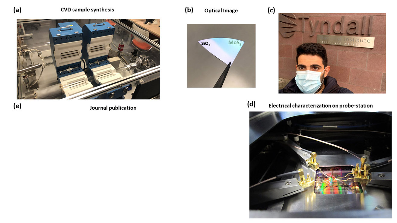
With the continuous collaboration of the three groups, we recently published several manuscripts (Figure e depicts the one showing the light-sensing of MoS2 devices, see Marquez et al., 2021) and others are being written. In this framework, we have recently received an invitation to contribute to one of the most important conferences on this topic (IEEE, IRDS and International Nanodevices Conference).
Mobility put to the COVID-19 challenge
The COVID-19 pandemic has brought difficulties in all aspects of daily life, and research is not an exception. Many researchers are worried about the challenges that the mobility restrictions have brought in these international actions. However, the contingency plan that was put together with the support of our collaborators and the European Commission MSCA board, has helped us in dealing with the actual limitations and creating new opportunities from the adversity.
I hope that this personal experience will help other researchers facing similar challenges.
Acknowledgements
I wish to express my gratitude to all the members of the three research teams involved in the progress of this MSCA (895322): Paul Hurley’s team at Tyndall National Institute, Ireland (special mention to Farzan Gity), Edward Chang’s group at National Yang Ming Chiao Tung University, Taiwan and to my host group, Francisco Gamiz’ team, at University of Granada, Spain. The European Commission and the Marie Curie officer board are thanked for their disposition to dynamically act against the issues that surged from the pandemic. This project has received funding from the European Union’s Horizon 2020 Research and Innovation Programme under the Marie Skłodowska-Curie grant agreement No 895322.
Carlos Marquez
Department of Electronics and CITIC-UGR,
University of Granada, Spain
carlosmg@ugr.es
References
Marquez, C., Salazar, N., Gity, F., Galdon, J. C., Navarro, C., Sampedro, C., Hurley, P. K., Chang, E. Y., & Gamiz, F. (2021). Hysteresis in As-Synthesized MoS2 Transistors: Origin and Sensing Perspectives. Micromachines, 12(6), 646. https://doi.org/10.3390/mi12060646